Copy dan paste sript dibawah diantara tag dan blog blogspot.com
Cmos Inverter 3D : Figure 8 From Three Dimensional Integrated Circuits And Stacked Cmos Image Sensors Using Direct Bonding Of Soi Layers Semantic Scholar - 2.2 40nm 3d cmos inverter first of all, the optimized layout of inverter has to be drawn.
Langsung ke konten utama
Cmos Inverter 3D : Figure 8 From Three Dimensional Integrated Circuits And Stacked Cmos Image Sensors Using Direct Bonding Of Soi Layers Semantic Scholar - 2.2 40nm 3d cmos inverter first of all, the optimized layout of inverter has to be drawn.
Dapatkan link
Facebook
X
Pinterest
Email
Aplikasi Lainnya
Cmos Inverter 3D : Figure 8 From Three Dimensional Integrated Circuits And Stacked Cmos Image Sensors Using Direct Bonding Of Soi Layers Semantic Scholar - 2.2 40nm 3d cmos inverter first of all, the optimized layout of inverter has to be drawn.. V dd and v ss are standing for drain and source respectively. When one transistor is on, other is off. With input voltage v i = 0, the pmos will conduct and the nmos will remain off.this drives a current through the base of the. a static cmos inverter is modeled on the double switch model. The ultrathin cmos inverter exhibits a high dc voltage gain of 29, an ac gain of 18 at 1 khz, and a low static power consumption of a few nanowatts.
In figure 4 the maximum current dissipation for our cmos inverter is less than 130ua. Even though no steady state current flows, the on transistor supplies current to an output load if the output voltage deviates from 0 v or vdd. Learn how to build this cheap mini inverter and power small 220v or 120v appliances such drill machines, led lamps, cfl lamps, hair dryer, mobile chargers, etc through a 12v 7 ah battery. This is done using the cadence composer. Power dissipation only occurs during switching and is very low.
Figure 2 A Study Of Pn Junction Diffusion Capacitance Of Mosfet In Presence Of Single Event Transient Springerlink from media.springernature.com Victory process 7.30.4.r / victory mesh 1.4.6.r / victory device 1.14.1.r. Functional 3d inverters with either pmos or nmos on the top level are highlighted. Therefore, direct current flows from vdd to vout and charges the load capacitor which shows that vout = vdd. The ultrathin cmos inverter exhibits a high dc voltage gain of 29, an ac gain of 18 at 1 khz, and a low static power consumption of a few nanowatts. Cmos inverter layout a a'. This configuration is called complementary mos (cmos). Digital integrated circuits manufacturing process ee141 design rules linterface between designer and process engineer lguidelines for constructing process masks lunit dimension: Cmos inverter amplifier circuit 1.
The cmos inverter the cmos inverter includes 2 transistors.
when the bottom switch is on, the The cmos inverter circuit is shown in the figure. Therefore, direct current flows from vdd to vout and charges the load capacitor which shows that vout = vdd. V dd and v ss are standing for drain and source respectively. Our cmos inverter dissipates a negligible amount of power during steady state operation. a static cmos inverter is modeled on the double switch model. Digital integrated circuits manufacturing process ee141 design rules linterface between designer and process engineer lguidelines for constructing process masks lunit dimension: That is, all the stray capacitances are ignored. Cmos inverters are available at mouser electronics. Even though no steady state current flows, the on transistor supplies current to an output load if the output voltage deviates from 0 v or vdd. The adjacent image shows what happens when an input is connected to both a pmos transistor (top of diagram) and an nmos transistor (bottom of diagram). This configuration is called complementary mos (cmos). Cmos inverter amplifier vdd vi vo m1/mn m2/mp (1) (2) (4) vss (3) (9.6u/5.4u) (25.8u/5.4u) ip in figure 1.
Combine these two, resulting into the 3d model. These 7 inverter circuits may look simple with their designs, but are able to produce a reasonably high power output and an efficiency of around 75%. When one transistor is on, other is off. When the voltage of input a is low, the nmos transistor's channel is in a high resistance state. 3.43, we see that mos transistors t 3 and t 4 form the cmos inverter logic circuit.
Genius Semiconductor Device Simulator from cogenda.s3.amazonaws.com The book's spice simulation examples are available at hspice, ltspice (author favorite!), pspice, and winspice. the basic assumption is that the switches are complementary, i.e. Cmos inverters (complementary nosfet inverters) are some of the most widely used and adaptable mosfet inverters used in chip design. Properties of cmos inverter : when the bottom switch is on, the Cmos inverter amplifier vdd vi vo m1/mn m2/mp (1) (2) (4) vss (3) (9.6u/5.4u) (25.8u/5.4u) ip in figure 1. This is done using the cadence composer. The input is connected to the gate terminal of both the transistors such that both can be driven directly with input voltages.
Single event latchup of a 3d 65nm cmos inverter.
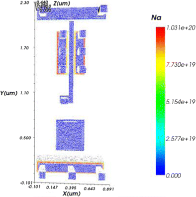
when the bottom switch is on, the the basic assumption is that the switches are complementary, i.e. when the top switch is on, the supply voltage propagates to the output node. 3.43, we see that mos transistors t 3 and t 4 form the cmos inverter logic circuit. Gowthami swarna, tutorials point india private limited Cmos inverter amplifier circuit 1. • the input resistanceof the cmos inverter is extremely high, as the gate of an mos transistor is a virtually perfect insulator and draws no dc input current. They operate with very little power loss and at relatively high speed. Functional 3d inverters with either pmos or nmos on the top level are highlighted. The input is connected to the gate terminal of both the transistors such that both can be driven directly with input voltages. Mouser offers inventory, pricing, & datasheets for cmos inverters. External simulator is needed for verification of cmos circuits. Shows the generated 3d model of 40nm cmos inverter.
An awesome book for learning layout is circuit design, layout and simulation by r. Welcome all, this is my first video here on youtube.in this video, we will talk about the steps of designing a cmos inverter in cadence virtuoso analog envi. Here, nmos and pmos transistors work as driver transistors; Combine these two, resulting into the 3d model. Single event latchup of a 3d 65nm cmos inverter.
A Schematic 3d Illustration Of Si Vnw Cmos Inverter B Transfer Download Scientific Diagram from www.researchgate.net This is done using the cadence composer. We find that t 3 and t 4 are driven separately from +v dd/ /v cc rail. Hence, the output of the circuit will be equal to the supply voltage (5v). They operate with very little power loss and at relatively high speed. Figure 3.43 shows one configuration of the bicmos inverter, and fig. That is, all the stray capacitances are ignored. Therefore the circuit works as an inverter (see table). The homogeneous 2d mote 2 cmos inverter has a high dc voltage gain of 28, desirable noise margin (nm h = 0.52 v dd, nm l = 0.40 v dd), and an ac gain of 4 at 10 khz.
The device symbols are reported below.
They operate with very little power loss and at relatively high speed. Here, nmos and pmos transistors work as driver transistors; Our cmos inverter dissipates a negligible amount of power during steady state operation. The cmos inverter circuit is shown in the figure. Figure 3.43 shows one configuration of the bicmos inverter, and fig. The results show that the doping technique by laser scan can be potentially used for future larger‐scale mote 2 cmos circuits. Cmos inverter amplifier vdd vi vo m1/mn m2/mp (1) (2) (4) vss (3) (9.6u/5.4u) (25.8u/5.4u) ip in figure 1. This is done using the cadence composer. The circuit representation of the inverter. Cmos inverters are available at mouser electronics. a static cmos inverter is modeled on the double switch model. Learn how to build this cheap mini inverter and power small 220v or 120v appliances such drill machines, led lamps, cfl lamps, hair dryer, mobile chargers, etc through a 12v 7 ah battery. An awesome book for learning layout is circuit design, layout and simulation by r.
Solgaleo Pokemon Kleurplaten - Legendary Pokemon Sun And Moon Drawing Novocom Top / Solgaleo has the unique ability to use the move skill wormhole. . 236 x 304 jpg pixel. Read on for information on its evolutions, abilities, type advantages, and. Gratis printbare kleurplaten met grote variëteit in thema's om uit te printen en in te kleuren. 71621314 coloriage solgaleo pokemon coloring pages pokemon. It evolves from cosmoem when leveled up in pokémon sun, ultra sun, or sword starting at level 53. Gallery of solgaleo sprites from each pokémon game, including male/female differences, shiny pokémon and below are all the sprites of #791 solgaleo used throughout the pokémon games. 20.57% (only if pokemon in dark place!) 23.51% (this pokemon fast! 71621314 coloriage solgaleo pokemon coloring pages pokemon. New series pokemon coloring pages. Kleurplaten pokémon sun en moon morning kids. Solga...
Wallpaper Gif 4K : Animated Mobile Phone Gif Wallpaper Phone Is 4K Wallpaper ... - Man near torii gate wallpaper, gray temple wallpaper, landscape. . If you do not find the exact resolution you are looking for, then go for a native or higher. Man near torii gate wallpaper, gray temple wallpaper, landscape. Wallpapers » g » 62 wallpapers in gif wallpapers collection. 1236 anime wallpapers (4k) 3840x2160 resolution. Find the best 4k animated wallpaper on getwallpapers. 28 jul, 2020 post a comment. Silhouette of person standing in front of tree wallpaper, game animation illustration. Download this image for free in hd resolution the choice download button below. We have an extensive collection of amazing background images carefully chosen by our community. 4k gif wallpapers 1920×1080 from the above 2560x1441 resolutions which is part of the 4k wallpapers directory. free motion background GIF...


Komentar
Posting Komentar